Flexible Printed Circuit (FPC) Design Guide: Bend Radius, Stack-up and Cost Drivers for OEMs
Most flex circuits do not fail on the engineering bench. They fail in the field, months later, when a hinge has folded tens of thousands of times and one copper trace finally opens. The layout passed every electrical check and the assembly fit the housing, yet the part still died - because flexible printed circuit reliability is mechanical before it is electrical. Bend radius, copper type and stack-up decide whether an FPC survives one installation fold or millions of motion cycles.
This FPC design guide covers the decisions in the order a design engineer meets them: when a flex circuit is the right interconnect at all, the strain physics behind every bend rule, static versus dynamic radius numbers, the material stack-up layer by layer, RA versus ED copper, bend-zone routing, ZIF tail and stiffener tolerances, and the cost drivers that move an FPC quote. Where numbers are quoted they follow commonly used fabricator guidance aligned with IPC-2223 - confirm final values against the standard and your supplier's process capability.
FPC Bend Rules at a Glance
- Static fold (bent once at assembly): minimum bend radius of 6 - 10 x total thickness for single-sided flex; 10 - 12 x for double-sided; 24 x for multilayer.
- Dynamic flex (moves in service): 20 - 40 x total thickness for single-sided constructions, 40 - 100 x for double-sided; avoid multilayer in the moving path.
- Copper choice: rolled-annealed (RA) copper in every dynamic path; electrodeposited (ED) copper is acceptable only in static folds.
- Bend zones: no vias, pads, stiffeners or trace width changes; route conductors perpendicular across the bend line.
When a Flexible Circuit Beats a Wire Harness - and When It Does Not
An FPC earns its place when at least one of three conditions is true. The connection crosses a moving joint - a hinge, a slider, a rotating print head. The routing space is thin - behind a display, inside a door panel, along a chassis wall. Or assembly labour matters - one laminated flex with a ZIF tail terminates in seconds, while a harness needs routing, dressing, strain relief and two or more connectors. Add repeatability: a flex folds the same way every time, which removes a whole class of harness assembly variation.
The honest counter-cases: high current that needs heavy copper, more than a few layers, impedance-controlled high-speed lines a rigid board already handles, or pure cost in a static connection - a harness or rigid board is usually cheaper there. FPCs also dislike being treated as cables: they are engineered structures with a defined bend axis, not ropes.
The Physics Behind Every Bend Rule: Neutral Axis and Copper Strain
Bend a stack-up and the outer surface stretches while the inner surface compresses. Somewhere between them sits the neutral axis, where strain is zero. Copper survives when it sits close to that axis and sees low strain; it work-hardens and cracks when it sits far from it under high strain. Every bend rule in this guide is that one goal in disguise: keep copper strain low. A larger radius, thinner copper and a single flex layer all pull the copper toward the neutral axis - which is why the same trace can last five hundred cycles or five million depending on geometry alone.
Static Versus Dynamic: Choosing the FPC Bend Radius
The first question is never "what radius" but "how many bends". A static flex is bent once during assembly and never moves again. A dynamic flex keeps moving in service - hinges, sliders, robotic heads. The distinction changes every downstream choice, because fatigue accumulates on every cycle.
| Construction | Static: minimum bend radius | Dynamic: minimum bend radius |
|---|---|---|
| Single-sided flex | 6 - 10 x total thickness | 20 - 40 x total thickness (up to 100 x for very high cycle counts) |
| Double-sided flex | 10 - 12 x total thickness | 40 - 100 x total thickness |
| Multilayer flex | 24 x total thickness | Generally not recommended in the moving path |
Two practical notes. First, the multipliers scale with total thickness, so every layer you add - stiffer coverlay, a thick stiffener nearby, heavy copper - pushes the required radius up. Second, radius buys cycle life exponentially, not linearly: opening a hinge radius from 4 mm to 8 mm can move a design from thousands of cycles into the millions. When a datasheet quotes a bend life, read the test conditions - cycle count, bend angle, dwell - before comparing it to your application.
The Material Stack-Up, Layer by Layer
A typical single-sided flex, from bottom to top: polyimide base film, adhesive (or none, in adhesiveless laminates), copper foil, coverlay openings over the pads, and surface finish on the exposed copper. The two decisions that shape everything else are the base film and the copper:
| Property | Polyimide (PI) | Polyester (PET) |
|---|---|---|
| Continuous service temperature | roughly 200°C class | roughly 105°C class |
| Survives solder reflow | Yes | No |
| Dynamic flex life | Excellent | Fair |
| Relative material cost | Several times PET | Baseline |
Any circuit that gets soldered or sees heat belongs on polyimide; PET is reserved for low-temperature, low-cost static circuits such as simple membrane tails. Common PI base film thicknesses are 12.5, 25 and 50 μm, and coverlay is typically 25 μm PI with a matching adhesive layer. Adhesiveless laminates - copper cast directly onto PI - remove the acrylic layer that softens during soldering, thin the stack (which improves the bend ratio) and are increasingly the default for high-reliability builds.
Copper Foil: RA Versus ED Copper
| Property | Rolled-annealed (RA) copper | Electrodeposited (ED) copper |
|---|---|---|
| Grain structure | Long grains aligned with the flex direction | Vertical columnar grains |
| Dynamic flex life | Excellent - the default for moving paths | Poor - grains are crack paths under repeated bending |
| Static folds and rigid-flex transitions | Suitable | Suitable and cost-effective |
| Typical thicknesses | 12 - 35 μm common; 70 μm for current | 12 - 70 μm |
| Relative cost | Higher | Lower |
For any dynamic application RA copper is not an upgrade; it is the design. Copper thickness is the trade-off: thinner copper sits closer to the neutral axis and flexes more freely, while heavier copper buys current capacity at the cost of bend life.
Bend-Zone Routing Rules
Inside the area that actually flexes, a short list of rules prevents most field failures:
- Route traces perpendicular across the bend line, never parallel to it, so strain spreads across the whole conductor instead of concentrating at its edge.
- Keep vias, plated through-holes, pads and stiffeners out of the bend zone entirely; they are crack initiation points.
- Avoid 90-degree corners and abrupt width changes in the bend; use radiused corners and teardrop transitions into pads.
- On double-sided dynamic flex, stagger top and bottom traces instead of stacking them, which keeps the section flexible.
- Leave the coverlay continuous across the bend zone; openings belong over pads, outside the flexing region.
Stiffeners, ZIF Tails and Connector Tolerances
Where the flex terminates, stiffness becomes a feature: ZIF connectors, SMT pads and screw-down points all need local support. FR-4 stiffeners are the default, polyimide stiffeners suit thin profiles, and stainless appears where the tail also acts structurally. Three details generate most of the rework in real programs:
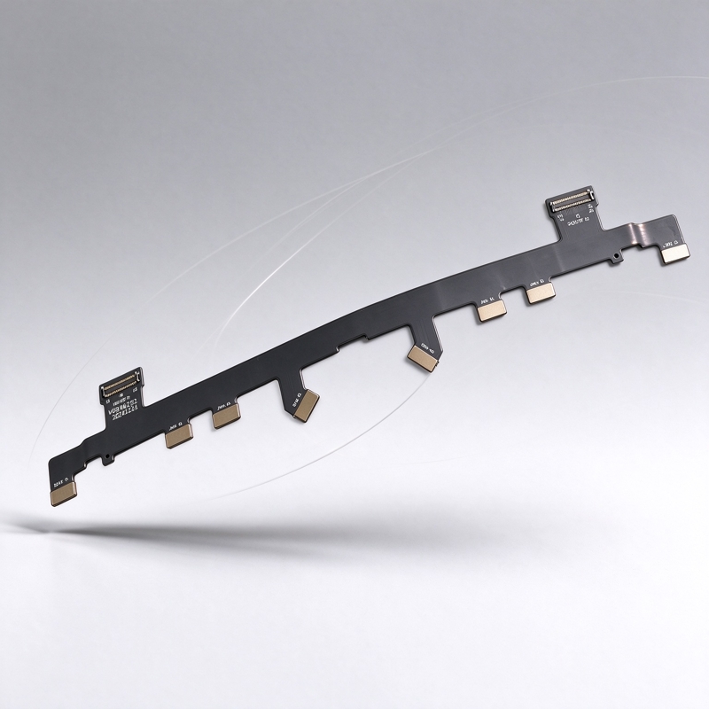
A production FPC with two ZIF termination tails and gold-plated contact fingers. Tail thickness and stiffener placement are controlled dimensions, not defaults.
- Tail thickness. ZIF connectors clamp to a window. Designs commonly target 0.20 mm or 0.30 mm nominal tail thickness with a tolerance around ±0.05 mm, but the number that matters is on the connector datasheet - design to it and hold the whole stack-up (base film, adhesive, copper, coverlay, stiffener) to that total.
- Stiffener position. Keep the stiffener edge clear of the bend zone, and size the contact area so the tail cannot rock in the connector. The stiffener sets insertion force and protects the fingers.
- Gold fingers. Contact fingers get a hard gold finish over nickel; insertion cycles and connector pitch (0.5 mm and 1.0 mm are the common ones) define pad geometry and plating thickness.
Shielding and Impedance on Flex
When the flex carries sensitive signals, shielding options trade flexibility against coverage: a solid copper plane shields best but stiffens the circuit, a hatched plane preserves most of the bending freedom - commonly cited around 40% more flexible than solid - and thin conductive shielding films applied over the coverlay save thickness. On impedance: polyimide's dielectric constant sits around 3.2 - 3.5 and dielectric layers are thin, so controlled-impedance lines on flex are calculated differently from FR-4; hatched reference planes must be included in the model, and the 3W spacing rule between parallel signals is a sensible default. Keep trace-to-plane spacing consistent along the whole signal path to avoid impedance discontinuities.
What Drives FPC Cost - and How to Control It
| Cost driver | Why it moves the price | How to control it |
|---|---|---|
| Base material | PI versus PET, RA versus ED copper, adhesiveless versus adhesive laminate | Specify PI and RA copper only where the application demands them |
| Layer count | Each layer adds lamination, drilling and registration cost | Route dynamically; keep the moving path single-layer |
| Line width / spacing | 0.10/0.10 mm is everyday capability; finer geometry narrows the supplier pool and panel yield | Widen traces wherever routing density allows |
| Surface finish | ENIG or OSP for SMT pads, hard gold over nickel for ZIF fingers | Gold only on contact fingers, not the whole circuit |
| Stiffeners and shielding | Count, material and coverage add handling steps | Consolidate stiffener sizes; shield only the sensitive runs |
| Electrical test | 100% fixture or flying-probe testing is standard for moving assemblies | Expect it - an untested flex is a field failure in transit |
| Order quantity and panel utilisation | Nesting efficiency is a quiet lever on piece price | Review outline shape and panel layout with the supplier early |
Tolerances worth specifying up front: die-cut outlines typically hold around ±0.10 - 0.20 mm (laser cutting holds tighter where the design needs it), coverlay openings around ±0.10 - 0.15 mm directly over fine-pitch pads, and hole-to-pad registration is weaker than on rigid board because the material moves during lamination - give pads the anchor area they need.
Pre-Quote DFM Checklist for Flexible Circuit Designs
Before sending an FPC out for quotation, a ten-minute internal review against this list usually removes a revision cycle:
- Classify every bend as static or dynamic, and note the cycle count for dynamic paths.
- Check each bend radius against the ratio table for the actual stack-up thickness.
- Confirm no vias, pads, stiffeners or width changes inside any bend zone.
- Verify traces cross bend lines at 90 degrees, with radiused corners and teardrops into pads.
- Confirm the tail thickness budget against the connector datasheet window.
- Decide shielding and impedance requirements up front, not after the first prototype.
- State the environment: temperature range, chemicals, UV, vibration.
- Define acceptance: IPC-6013 class, electrical test coverage, bend-cycle qualification method.
Qualifying an FPC Supplier
The questions that separate a flex-capable manufacturer from a brochure: Which IPC-6013 class do you build and test to? Is 100% electrical test standard, and can you show coverage for a recent lot? Can you provide bend-cycle and thermal-cycling data on a construction like mine? How do you control coverlay registration over fine-pitch tails? Where do material certifications and batch traceability come from - a supplier spreadsheet or an in-house MES record?
KeypadOne is the brand of Dongguan Zhongjia Printing Co., Ltd., a precision manufacturer founded in 2009 with a 20,000 m² facility in Dongguan, China. FPC and membrane switch circuits are produced alongside each other - which matters when a control panel needs the switch, the flex tail and the nameplate integrated as one assembly - with about 30 R&D engineers and a quality team of around 90 running in-house electrical testing on dedicated PCB short-circuit testers, plus CCD vision inspection, peel testing and thermal-cycling chambers. Certifications include ISO 9001:2015, IATF 16949:2016 and QC 080000:2017, with RoHS, REACH, SGS and UL documentation on selected products, and ERP + MES batch traceability from material receipt to shipment. See the FPC solutions page, the integrated membrane switch solutions overview, or route a drawing through the inquiry page for a stack-up proposal and quotation.
Key Takeaways
- Classify bends first: a static fold and a dynamic hinge are different engineering problems with different rules.
- Every bend rule protects one thing - low copper strain at the neutral axis. Radius, copper type and stack-up thickness are the three levers.
- RA copper is mandatory in dynamic paths; ED copper is acceptable in static folds.
- Keep vias, pads and stiffeners out of bend zones and route traces perpendicular to the bend line.
- Tail thickness, stiffener position and gold-finger finish are connector-driven dimensions: design to the connector datasheet.
- When comparing quotes, weigh test coverage and traceability with the piece price. KeypadOne's quality and certification documentation is available on request with any quotation.
FPC Design FAQ
What bend radius should I use for a dynamic flex?
Start from the ratio table: 20 - 40 x total thickness for single-sided dynamic flex, more for double-sided, and avoid multilayer in the moving path. For very high cycle counts, work toward 100 x. Then qualify with a bend-cycle test on the real construction - the ratio is a design floor, not a guarantee, and cycle life rises exponentially with radius.
When is ED copper acceptable instead of RA copper?
In static applications: a fold-to-install bend, a rigid-flex transition, or a flex that never moves after assembly. ED copper's vertical grain structure cracks along grain boundaries under repeated strain, which is why rolled-annealed copper is the default for anything that flexes in service.
Can I put a via inside the bend area if it is small?
No. Vias, plated holes and pads are stress concentrators and the most common crack initiation points in bend zones. Move the via outside the bend and route the connection perpendicular across it - the detour costs almost nothing in area and removes a whole failure mode.
PI or PET for my application?
If the circuit is soldered, sees reflow or any sustained heat, it is PI. PET suits low-cost, low-temperature, static circuits - simple membrane tails and disposable devices. A PET circuit that cannot survive the assembly process is scrap before it ships, so the material decision is usually made by the soldering process, not by preference.
What information should an FPC quotation include?
A stack-up proposal with thicknesses, the bend-radius table applied to your actual geometry, electrical test coverage, IPC-6013 class, material certifications, and the lead time for first articles. If a quote returns a price without a stack-up or a test plan, the price is not comparable - the missing engineering will reappear as revisions later.